
Taiwan Semiconductor Manufacturing Company
The world's most important company you can't replace

Executive Summary
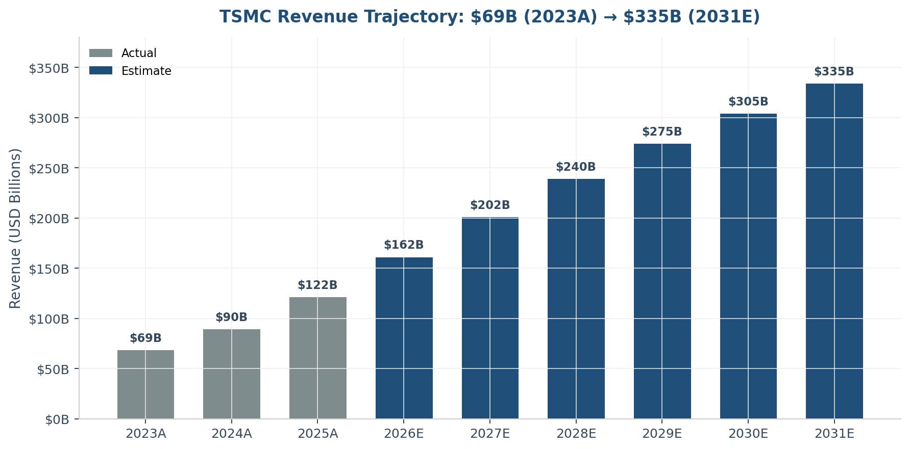
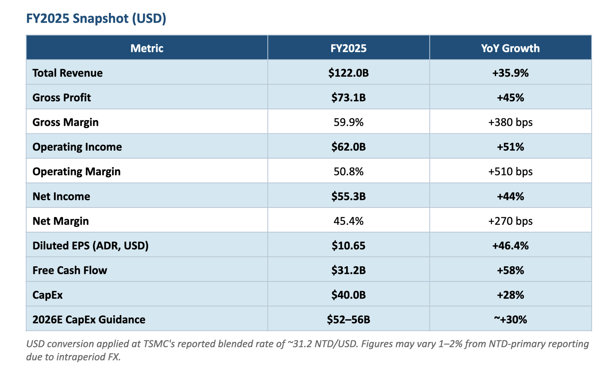
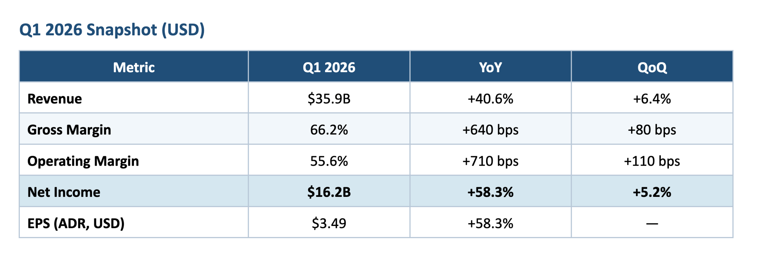
Taiwan Semiconductor Manufacturing Company (TSMC) closed fiscal 2025 with $122 billion in revenue — up 35.9% in U.S. dollar terms — and followed it with a blistering Q1 2026, posting $35.9 billion in revenue (+40.6% YoY) and a 66.2% gross margin. Management now guides full-year 2026 revenue to grow more than 30% in USD, an unprecedented trajectory for a company of this scale. The foundry that Morris Chang built from $220 million in seed capital in 1987 is now the single most important bottleneck in the global AI build-out, and its operating performance reflects that fact.
Key Metric: TSMC controls ~60% of the global foundry market and ~90% of leading-edge (≤7nm) foundry market share. No competitor is closer than 18 months behind on nodes that matter for AI and flagship smartphones.
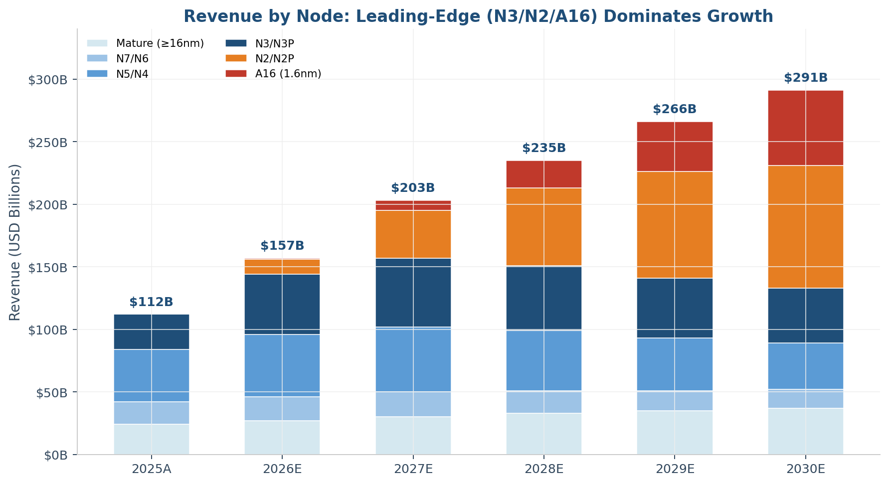
TSMC’s business has fundamentally transformed. For the first time in more than a decade, Nvidia — not Apple — is the company’s largest customer, accounting for roughly 19% of 2025 revenue and projected at 22% in 2026 (approximately $35 billion). High-Performance Computing (HPC), which captures Nvidia, AMD, Broadcom, and the hyperscaler ASIC programs, now represents 55–59% of revenue, up from 43% just two years ago. The 3nm node alone delivered 28% of Q4 2025 revenue — a node that did not exist commercially 30 months ago. And 2nm, which entered mass production in Q1 2026, is already booked through 2028 at 78–104 week lead times.
The thesis is straightforward: TSMC is the only company in the world that can manufacture leading-edge logic at scale, and the demand curve for leading-edge logic has been structurally reset higher by generative AI. The financial consequences — 50.8% operating margins, $122B+ run-rate revenue, and capex guided to $52–56B in 2026 — are visible in the numbers. The open questions are how long the runway lasts, how much margin expansion remains, and how to price the geopolitical risk embedded in the stock.
Key Metric: TSMC's Q1 2026 gross margin of 66.2% is the highest in its history and roughly 1,300 bps above management's long-run structural target of 53%. Mix shift toward 3nm and CoWoS has permanently reset the margin floor higher.
1. Origins: Morris Chang and the Invention of the Foundry Model
1.1 The Man Before the Company
Morris Chang’s story does not begin in Taiwan. Born in Ningbo, China in 1931, Chang fled the Japanese invasion and later the communist takeover before arriving in the United States in 1949. He earned bachelor’s and master’s degrees in mechanical engineering from MIT, was rejected from MIT’s doctoral program, and took a job in 1955 at Sylvania Semiconductor, where he learned by doing. In 1958 he joined Texas Instruments, where he would spend the next 25 years of his career. He completed a PhD in electrical engineering at Stanford in 1964 while working full-time, and rose to become a Group Vice President in charge of TI’s entire global semiconductor business — the third-ranking executive in the company.
Chang is widely credited as the first executive in the industry to apply the economic logic of the experience curve to semiconductor pricing: price below current cost, drive volume, ride the learning curve down, and capture share. This was unorthodox at the time. It became the foundation of Texas Instruments’ dominance in the 1960s and 1970s, and it would later become the operational DNA of TSMC.
By the early 1980s Chang had been passed over for the TI CEO job. He left for General Instrument in 1983, but the fit was poor and he resigned within a year. At 54 years old, in possession of one of the most distinguished operating records in the industry, Chang was effectively unemployed.
1.2 The Call From Taiwan
In 1985, Taiwan’s premier Sun Yun-suan and K.T. Li, the minister without portfolio who was the architect of Taiwan’s industrial policy, asked Chang to return to Taiwan and lead the Industrial Technology Research Institute (ITRI). Taiwan had been trying to build a domestic semiconductor industry for a decade with mixed success. Chang accepted, reasoning that his highest-impact work might be outside the United States rather than inside it.
Two years later, in February 1987, Chang — now 56 — founded Taiwan Semiconductor Manufacturing Company with US$220 million in seed capital. The Taiwanese government provided roughly 48% of the funding, Dutch electronics giant Philips provided 27.5% (along with critical process technology licenses), and private Taiwanese investors supplied the remainder. Chang himself put almost no personal capital in; what he brought was credibility, operational skill, and a single heretical idea.
1.3 The Idea
Every semiconductor company in the world in 1987 was integrated. Intel designed chips and fabricated them. Texas Instruments designed chips and fabricated them. Motorola, National Semiconductor, AMD, IBM — all of them owned their fabs. The reason was simple: fabs were where the hard engineering lived, and a company that gave up its fab gave up its ability to innovate at the physical level.
Chang’s insight was that this logic was breaking down. The cost of a leading-edge fab had crossed $200 million and was rising geometrically. Utilization rates at integrated device manufacturers (IDMs) were chronically poor because design cycles and fab cycles did not line up. Meanwhile, a new generation of engineers — people like Jen-Hsun Huang, Irwin Jacobs, and a handful of Silicon Valley designers — wanted to start chip companies but could not afford to build fabs. If someone would manufacture for them on contract, without competing with them, an entire new industry could be born.
Chang proposed to be that someone. TSMC’s founding principle was that it would never design its own chips, never compete with its customers, and never prioritize one customer over another. This neutrality, which sounds mundane now, was revolutionary then. It allowed a fabless semiconductor industry to exist, which in turn allowed Nvidia (founded 1993), Qualcomm (1985 but took off in the 1990s), Broadcom (1991), and eventually Apple’s silicon team to exist as serious businesses.
The early years were hard. TSMC’s first process node was two generations behind Intel. Its first major customer wins came from second-tier design houses that the IDMs would not serve. But the model worked. By 1994 TSMC went public. By 2000 it had passed UMC to become the dominant pure-play foundry. By 2010 it had passed Globalfoundries and was pulling away from everyone. By 2020 it was manufacturing nearly every smartphone SoC on the planet, and Intel — once the undisputed king of process leadership — was publicly acknowledging that it had fallen behind.
Chang retired for the first time in 2005, came back in 2009 when the company was hit hard by the financial crisis, shepherded the push to 28nm and then to 16nm FinFET, and finally stepped down for good in 2018 at age 87. He had personally overseen every major technology transition from the company’s founding through the introduction of 7nm. When he left, TSMC was worth roughly $230 billion. Today it is worth $1.92 trillion — a roughly 8x return in seven years, during which the company’s share of leading-edge logic has only grown.
2. The Technology Stack
2.1 Process Nodes: Where the Revenue Comes From
TSMC reports wafer revenue by technology node, and the breakdown tells the story of where the industry is and where it is going. The following are Q1 2026 figures.
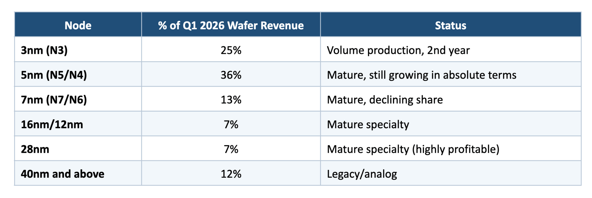
Key Metric: Advanced nodes (≤7nm) represented 74% of Q1 2026 wafer revenue, up from 69% a year ago. The ≤5nm bucket alone is 61% of revenue, up from 53%.
This mix shift is the single most important driver of TSMC's gross margin expansion from 53.1% in 2023 to 66.2% in Q1 2026. Leading-edge (N3/N2/A16) drives incremental growth while mature nodes remain a stable contributor.
2.2 3nm (N3): The Current Profit Engine
TSMC’s N3 family entered volume production in late 2022, with the N3E variant becoming the workhorse in 2024. In Q4 2025, 3nm accounted for 28% of revenue — the highest share any single node has ever reached in TSMC’s history at this point in its ramp. The node is structurally more profitable than its predecessors because Apple’s A17, A18, M3 and M4 families are fabricated on N3 (with Apple subsidizing the initial yield ramp through premium wafer pricing); wafer ASPs on N3 are roughly 25–30% higher than on N5 because of the additional EUV layers, with unit yields now above 80% on the N3E variant; and Nvidia’s GB200/GB300 Blackwell GPUs, AMD’s MI350 and Instinct series, and Broadcom’s Google TPU v6/v7 and Meta MTIA chips all sit on some flavor of N3 or N3P.
Approximately 55–60% of N3 wafer volume still goes to Apple in 2026, but the HPC share on N3 has grown rapidly — Nvidia alone will consume an estimated 18–22% of N3 capacity in 2026, with AMD, Broadcom, Marvell, and Meta rounding out another 15% collectively.
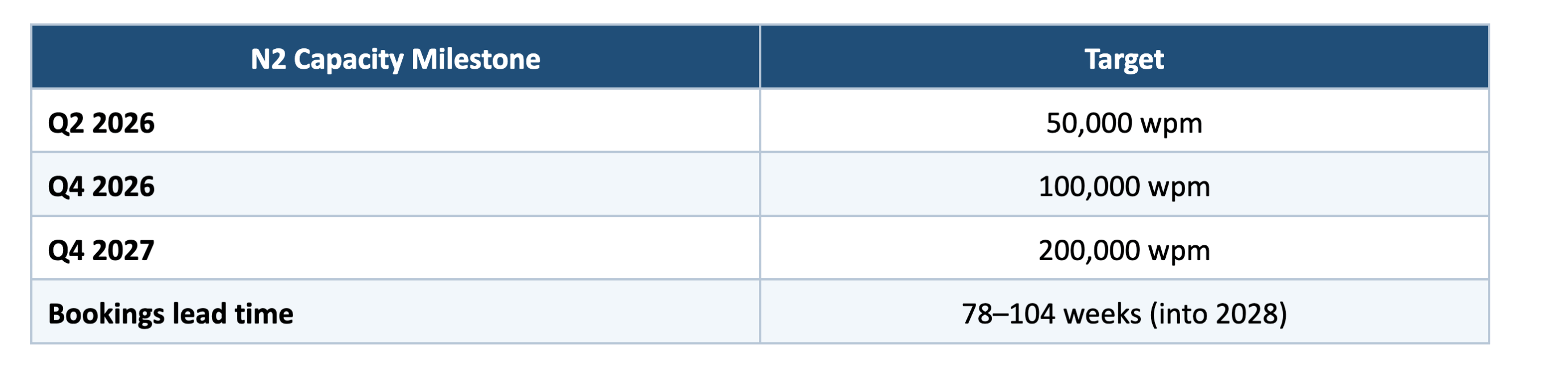
2.3 2nm (N2): The Next Growth Engine
TSMC began volume production of N2 in Q1 2026. N2 is the first TSMC node to abandon FinFET and move to Gate-All-Around (GAA) nanosheet transistors, which provide superior electrostatic control and enable roughly 15% higher performance at the same power or 25–30% lower power at the same frequency versus N3.
Apple is estimated to hold roughly 48–50% of the initial 2026–2027 N2 wafer allocation — its A20 iPhone SoC will be the first N2 product to ship at volume, in the fall 2026 iPhone 18 Pro. Nvidia, AMD, MediaTek, Qualcomm, Bitmain, and Google are confirmed N2 customers; Intel's planned Panther Lake tile will skip TSMC N2 in favor of its own Intel 18A, but its client GPU and data center accelerator lines will almost certainly move to N2 by 2027.
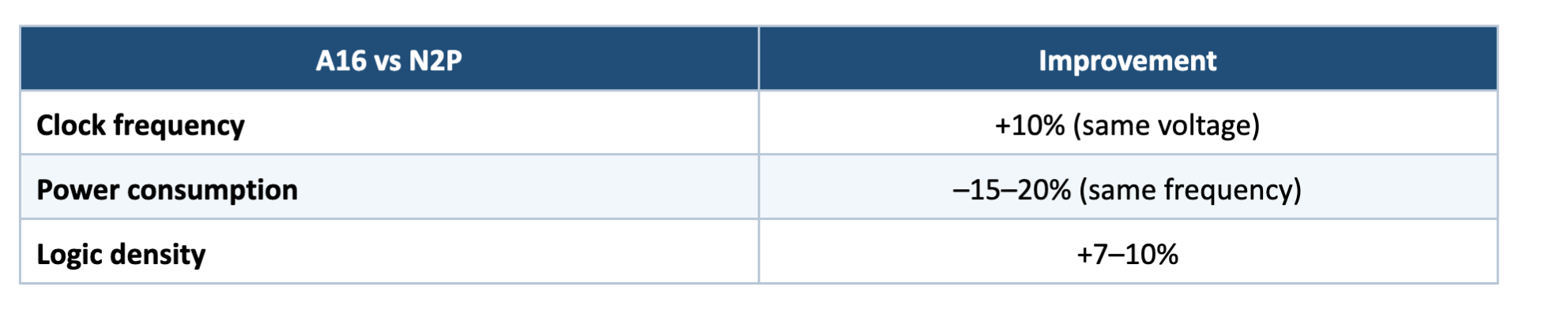
2.4 A16: The 1.6nm Angstrom Node
TSMC's A16 process, scheduled for volume production in H2 2026, marks the company's entry into the Angstrom era. A16 pairs nanosheet GAA transistors with a backside power delivery network that TSMC calls Super Power Rail (SPR). Backside power delivery moves the VDD/VSS rails to the wafer's reverse side, freeing up front-side routing for signal wiring — a critical improvement for the massively complex power delivery networks required by large AI accelerators.
A16 is explicitly positioned for AI and HPC workloads where both signal complexity and power density are extreme. Nvidia's next-generation Feynman architecture (following Rubin) is widely expected to be the first large-die A16 design, with tapeouts in 2027 and production silicon in 2028.
2.5 Advanced Packaging: CoWoS and the AI Bottleneck
Wafer fabrication is only half the story. Modern AI accelerators — Nvidia's Blackwell, AMD's MI355X, Google's TPU v7, AWS Trainium3 — are not monolithic dies. They are chiplet assemblies that integrate two to four logic dies with eight to twelve stacks of High Bandwidth Memory (HBM) on a single silicon interposer. The packaging technology that makes this possible is called CoWoS (Chip-on-Wafer-on-Substrate), and TSMC has a near-monopoly on it.
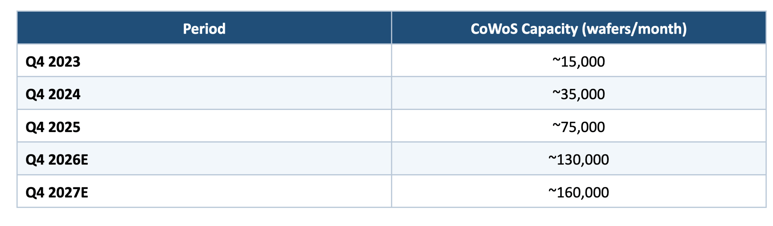
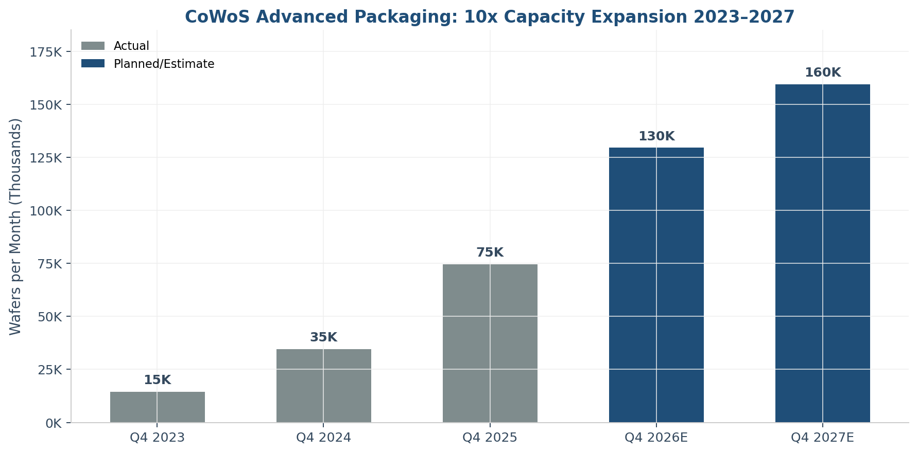
Key Metric: Nvidia alone has booked 60% of TSMC’s 2026 CoWoS allocation — roughly 800,000–850,000 wafer equivalents for the full year — to support volume Blackwell production and the Rubin (R100) ramp.
Broadcom (Google TPU, Meta MTIA), AMD, AWS (Trainium), and Microsoft (Maia) collectively consume another 25–30%. Fewer than one in ten CoWoS wafers is available for anyone else — including the entire non-AI HPC market.
The economic implication is that CoWoS is not a commodity; it is a differentiator. Wafer-equivalent pricing for CoWoS-L (the variant used for Blackwell and Rubin) is 3–5x that of a standard logic wafer. CoWoS alone contributes an estimated $14–17 billion in 2026 revenue, growing to $25–30 billion by 2028, with gross margins well above the corporate average.
2.6 SoIC: The Frontier Beyond CoWoS
Beyond 2.5D packaging, TSMC has been aggressively ramping 3D stacked silicon via its SoIC (System on Integrated Chips) technology. SoIC replaces the silicon interposer with direct copper-to-copper bonding between stacked dies, delivering 10x the connection density of CoWoS at lower power. Apple's M5 chip in late 2025 was the first high-volume commercial SoIC product. AMD's next-generation X3D server CPUs and Nvidia's Rubin Ultra (2027) are planned SoIC customers. The total 3D packaging revenue is still modest ($2–3B annualized as of Q1 2026) but is growing at triple-digit rates and is strategically the hedge against any future competitor cracking CoWoS.
2.7 The Moat in One Paragraph
The combination of N3, N2, A16, CoWoS, and SoIC — owned end-to-end by a single company with 60%+ of the foundry market and 90%+ of the leading-edge market — is the deepest and widest moat in the semiconductor industry since Intel's 1995–2005 dominance of the x86 ecosystem. A new entrant would need to raise $200+ billion in capex, license or develop EUV lithography, co-develop process recipes with ASML and dozens of materials suppliers, build a multi-decade-long operating learning curve, and convince the world's largest fabless customers to share their designs with an unproven foundry. None of that is going to happen on a reasonable investment horizon.
3. The Customer Stack: Who Actually Pays for 3nm and 2nm
TSMC does not publish customer-level revenue, but the data from analyst estimates, supply-chain tracking, and company disclosures converges tightly. Here is the best available picture of 2025 actuals and 2026 estimates.
3.1 Top 10 Customers (Estimated)
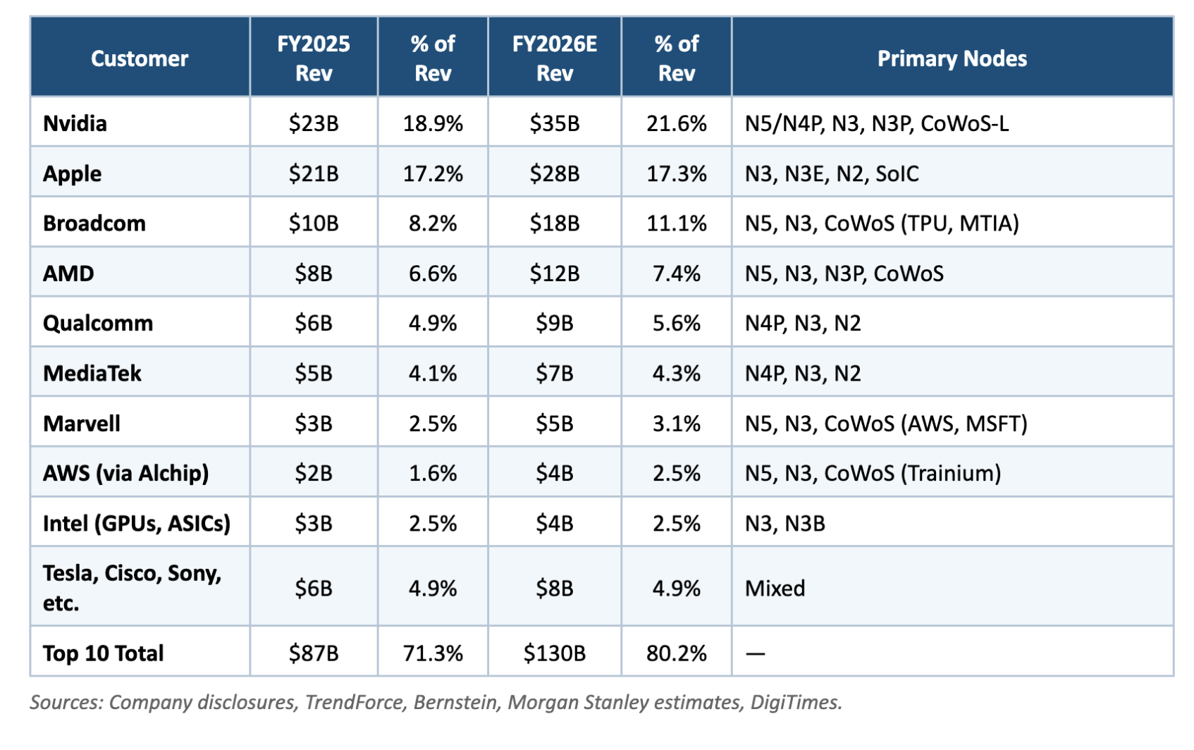
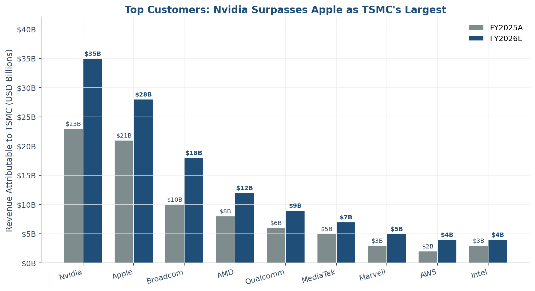
Key Metric: For the first time since 2014, Nvidia — not Apple — is TSMC’s largest customer. At a projected $35B in 2026, Nvidia alone is a bigger business inside TSMC than the entire TSMC of 2015 ($26B).
Nvidia has displaced Apple as TSMC’s largest customer. Apple’s unit volumes are relatively flat while iPhone ASPs are pressured, while Nvidia’s data center GPU revenue more than doubled in 2025. Blackwell silicon content per GPU is roughly 8–10x that of Apple’s A18 — a single B200 contains two massive N4P logic dies plus eight stacks of HBM plus a CoWoS-L interposer, versus a single relatively small Apple A18 die. At the wafer level, Apple still consumes more wafer starts than Nvidia, but on a revenue basis Nvidia has pulled ahead and will widen that lead in 2026.
Broadcom is the fastest-growing top-5 customer, primarily a function of the hyperscaler custom ASIC business. Broadcom designs and manufactures Google’s TPU v6 and v7, Meta’s MTIA v2, and is widely rumored to be building the next-generation OpenAI custom accelerator announced in 2025. Every one of these chips is fabricated on TSMC N3 or N3P and packaged in CoWoS-L. Broadcom’s TSMC spend is projected to rise from $10B in 2025 to $18B in 2026 — an 80% year-over-year jump.
Customer concentration has increased, not decreased, through the AI cycle. The top 5 customers represented roughly 52% of revenue in 2023 and will represent 63% in 2026. This is the inverse of the diversification that TSMC has historically talked up, and it is a meaningful risk factor.
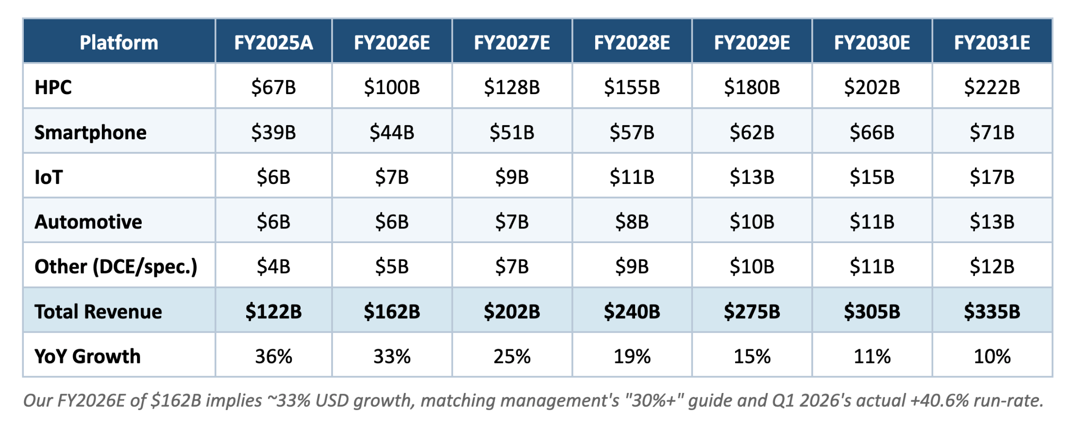
3.2 Platform Mix: HPC Has Eaten Everything
TSMC reports revenue by end-market platform. The shift over the past three years is stark:
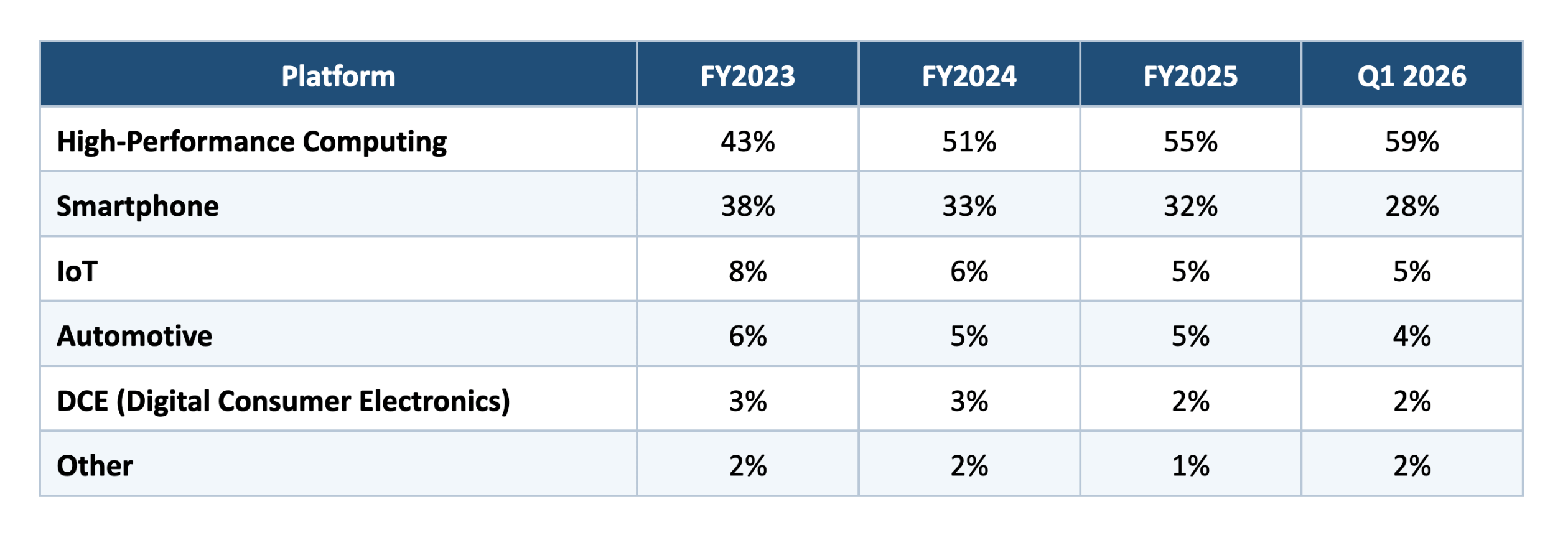
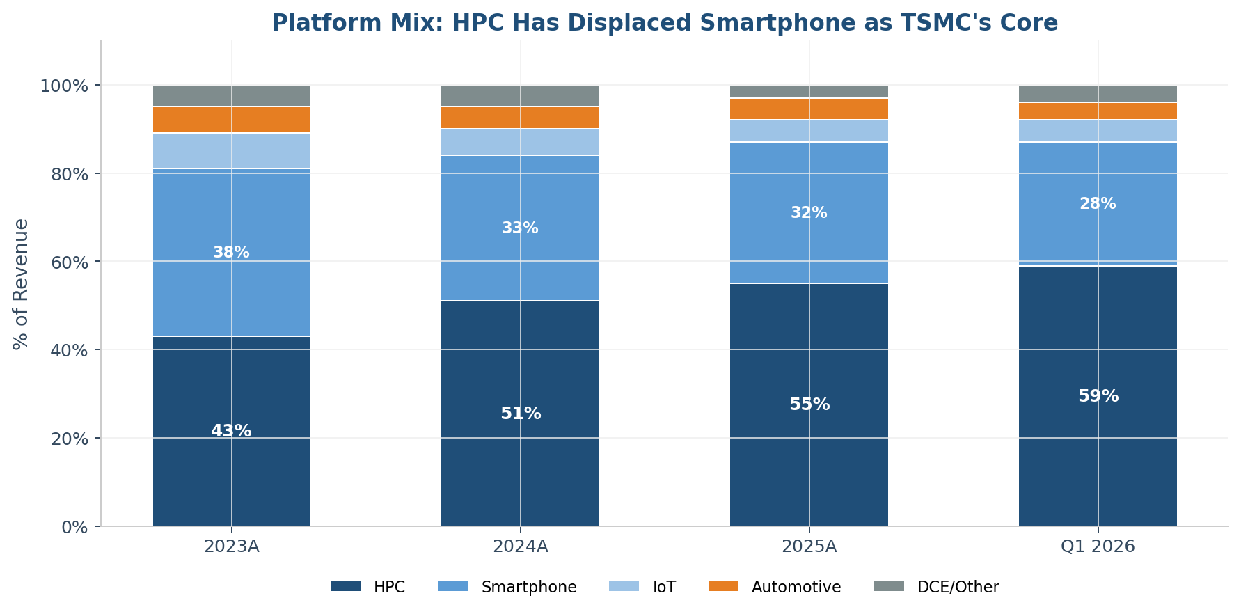
HPC now drives a clear majority of TSMC revenue, and the trend is still accelerating. Smartphone — which was the largest platform as recently as 2023 — has ceded primacy. This matters for valuation because HPC revenue carries higher wafer ASPs (particularly when bundled with CoWoS), has a longer design-to-revenue cycle that provides visibility, and is less seasonal than the smartphone-led business of the 2010s.
3.3 The API Capex Feedback Loop
The demand on TSMC is not random; it is the result of an identifiable and auditable capital cycle. The four largest U.S. hyperscalers — Amazon, Microsoft, Google, and Meta — collectively guided 2026 capex to approximately $640 billion, of which an estimated 55–60% is AI infrastructure. Roughly 70% of that AI capex ends up as Nvidia GPUs or custom ASICs (Google TPU, Meta MTIA, Microsoft Maia, AWS Trainium). Nearly 100% of those accelerators are manufactured by TSMC.
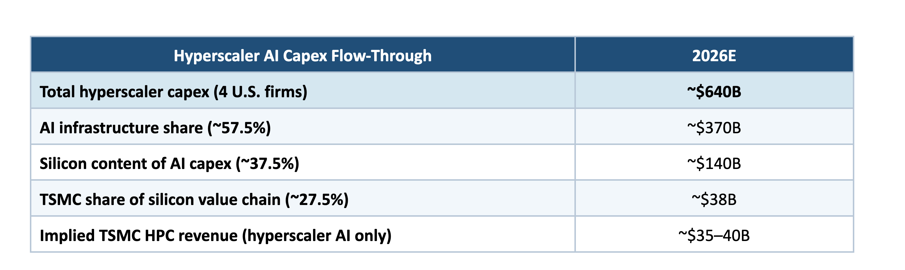
Key Metric: Roughly one-quarter of TSMC’s projected 2026 revenue comes from just four U.S. hyperscalers’ AI capex. The remaining three-quarters is Apple, Chinese hyperscalers, smartphone OEMs, automotive, and the long tail of specialty silicon.
This is the demand feedback loop that our AI Compute Demand report identified as the structural backbone of the sector: Nvidia's $192B FY2026 data center revenue projection, scaling toward $250–280B in FY2027, maps almost directly onto TSMC's CoWoS and N3/N2 allocations. The same capex dollars flow through Broadcom (TPU/MTIA), AMD, Marvell, and the custom-ASIC layer — all ultimately landing at TSMC.
4. Geopolitical Resilience: From Taiwan-Only to Global Footprint
4.1 The Arizona Build-Out ($165 Committed)
TSMC’s response to the Taiwan concentration risk is no longer theoretical. As of April 2026, TSMC has committed $165 billion to its Arizona campus in Phoenix — the single largest greenfield foreign direct investment in U.S. history. The scope now encompasses six fabrication facilities, two advanced packaging plants, and a major R&D center, with a total of twelve planned manufacturing modules by completion.
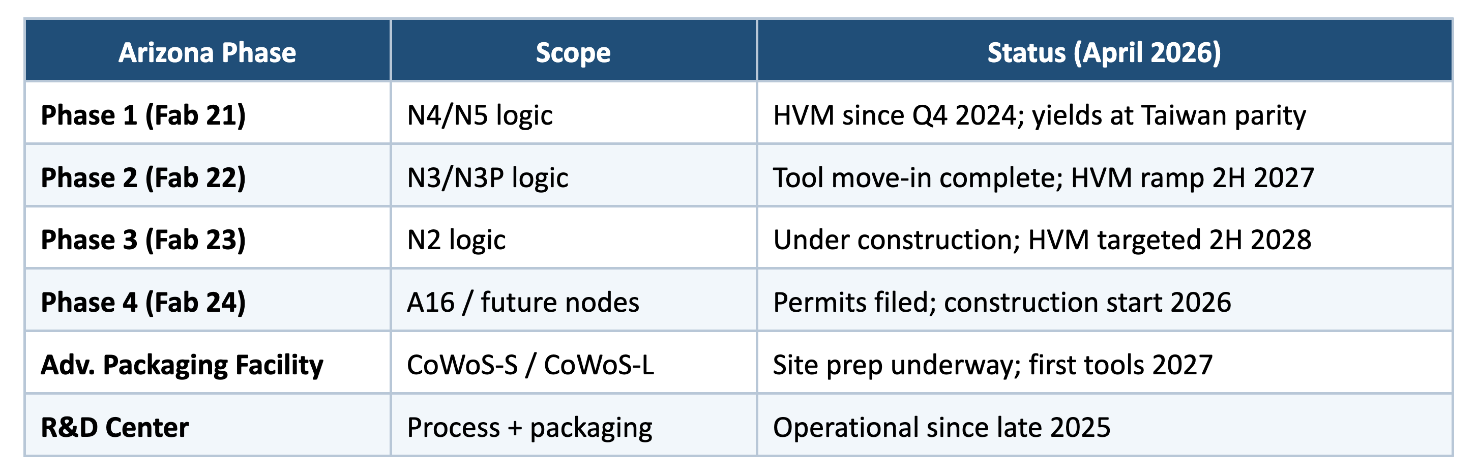
The economic and strategic implications are substantial. By year-end 2027, TSMC Arizona will be running N4 and N3 at roughly 50,000 wafers per month combined — approximately 4–5% of TSMC's global leading-edge wafer output, rising to an estimated 15% by 2030 as Phases 3 and 4 ramp. Critically, by late 2028 the Arizona packaging facility will begin localizing CoWoS assembly for U.S.-bound Nvidia, AMD, and hyperscaler ASIC volumes — closing the one remaining single-point-of-failure in the AI supply chain.
Key Metric: By 2030, roughly 20% of TSMC's leading-edge logic output and 10–15% of its advanced packaging capacity will be produced outside Taiwan — versus essentially 0% in 2023.
Arizona still carries a 200–300 bps gross margin dilution relative to Taiwan domestic fabs due to higher labor, construction, and operating costs. That gap has narrowed modestly through 2025 as Phase 1 yields reached Taiwan parity faster than expected. Management's internal target is to close the gap to 100–150 bps by 2029 as volume ramps and the local supplier ecosystem matures. Apple, Nvidia, AMD, and Qualcomm have all publicly committed to sourcing Arizona-fabricated silicon where available, and Apple has contracted ~40% of its U.S.-bound A-series wafer demand out of Arizona beginning in 2027.
4.2 Japan: Kumamoto’s Quiet Success
TSMC’s first Japan fab, JASM (TSMC-Sony-Denso JV) in Kumamoto, has been in high-volume production of 12/16/22/28nm specialty logic since early 2024. A second Kumamoto fab began installation in late 2025 and will add 7nm and 6nm capacity in 2027. The Japanese government has provided subsidies covering roughly 40% of the total ~$20B investment. Kumamoto now serves Sony’s image sensor business, the automotive tier-ones, and a range of specialty compute customers. It is the most margin-dilutive of TSMC’s overseas sites but strategically hedges Japanese automotive and imaging supply.
4.3 Germany: Dresden’s European Anchor
TSMC’s Dresden fab, a joint venture with Bosch, Infineon, and NXP known as ESMC, began construction in August 2024 and is scheduled for high-volume production in late 2027. Focused on 22/28nm and 12/16nm specialty logic for automotive and industrial applications, the facility is underwritten by €5 billion in German government subsidies out of a total €10 billion investment. Dresden is small in TSMC’s overall capacity footprint (~40,000 wafers/month at full ramp) but politically crucial — it de-risks European Union supply for the automotive industry and builds political cover for broader TSMC operations.
4.4 What This Means for the Taiwan Risk
In 2023, a Taiwan Strait disruption would have taken essentially 100% of TSMC’s output offline and with it the vast majority of global leading-edge logic. By 2028–2030, that single-point-of-failure posture changes materially:
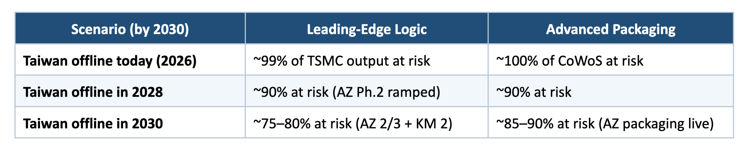
This is not a complete mitigation — Taiwan will remain the vast majority of TSMC's capacity for decades. But the direction of travel is meaningful and the pace is accelerating. A geopolitical event in 2030 would still be catastrophic for the global economy, but it would no longer be an existential event for TSMC as a corporate entity or for the leading-edge customers who rely on it. That progression should, over time, compress the Taiwan-risk discount embedded in the stock's multiple.
5. Financial Projections: 2026-2031
5.1 Methodology Note: Anchoring to the AI Compute Demand Curve
Our projections are explicitly informed by the trajectory established in our prior AI Compute Demand report. The foundational assumptions we carry forward: global AI infrastructure spend of $155B (2023) scaling to $635–690B (2026) and ~$1T (2028) — a 30%+ CAGR through 2028; Nvidia data center trajectory of $192B (FY26) → $250–280B (FY27), with the Blackwell-to-Rubin transition maintaining a multi-year backlog; AI accelerator share of TSMC revenue rising from 17–19% (2025) to 22–25% (2026) to 28–30% (2027); and hyperscaler AI capex flowthrough of 55–60% of $640B hyperscaler capex in 2026, with Amazon alone at $145–155B and Microsoft at $125–135B.
These inputs align with management's "30%+ USD revenue growth in 2026" guide. They also align with the Amazon Deep Dive assumption that AWS capex steady-state exceeds $110B annually through 2028 — meaningfully higher than consensus at the time that report was written.
5.2 Revenue Projections by Platform
Our base case assumes HPC grows at 38% in 2026 (tracking management's guide) and decelerates to mid-teens by 2031, tracking the hyperscaler capex curve; Smartphone grows in the mid-to-high single digits, driven primarily by 2nm unit ASP uplift; and the remaining platforms grow in line with global semiconductor demand.
5.3 Margin Projections
The key debate on TSMC is whether the Q1 2026 gross margin of 66.2% is the new normal or a cyclical peak. Our base case assumes gross margin expands modestly to a 63–67% range through the cycle (overseas fabs diluting roughly 200–300 bps versus the 68%+ domestic margin baseline); operating margin expands from 50.8% in FY2025 to 55.5% by 2027 before declining modestly to 52.5% by 2031 as overseas fab depreciation layers in; and net income margin tracks operating margin roughly 1:1 given stable interest income and effective tax rates in the 14–15% range.
6. Valuation: Discounted Cash Flow (DCF) Model
6.1 Key Assumptions
Note the WACC is 9.0% — matching the discount rate used in our Amazon Deep Dive. The rationale: TSMC's cash flow visibility has meaningfully improved (2nm bookings now extend to 2028), and the accelerating US/Japan/Germany footprint compresses the Taiwan-specific risk premium by roughly 50 bps. We retain a small premium versus pure U.S. mega-cap peers.
6.2 Free Cash Flow Projections (Unlevered)
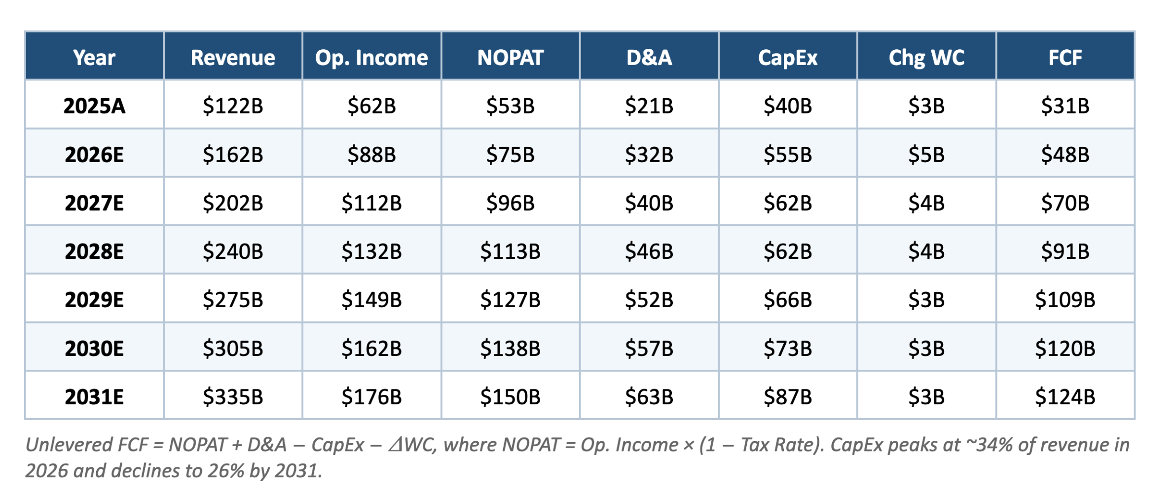
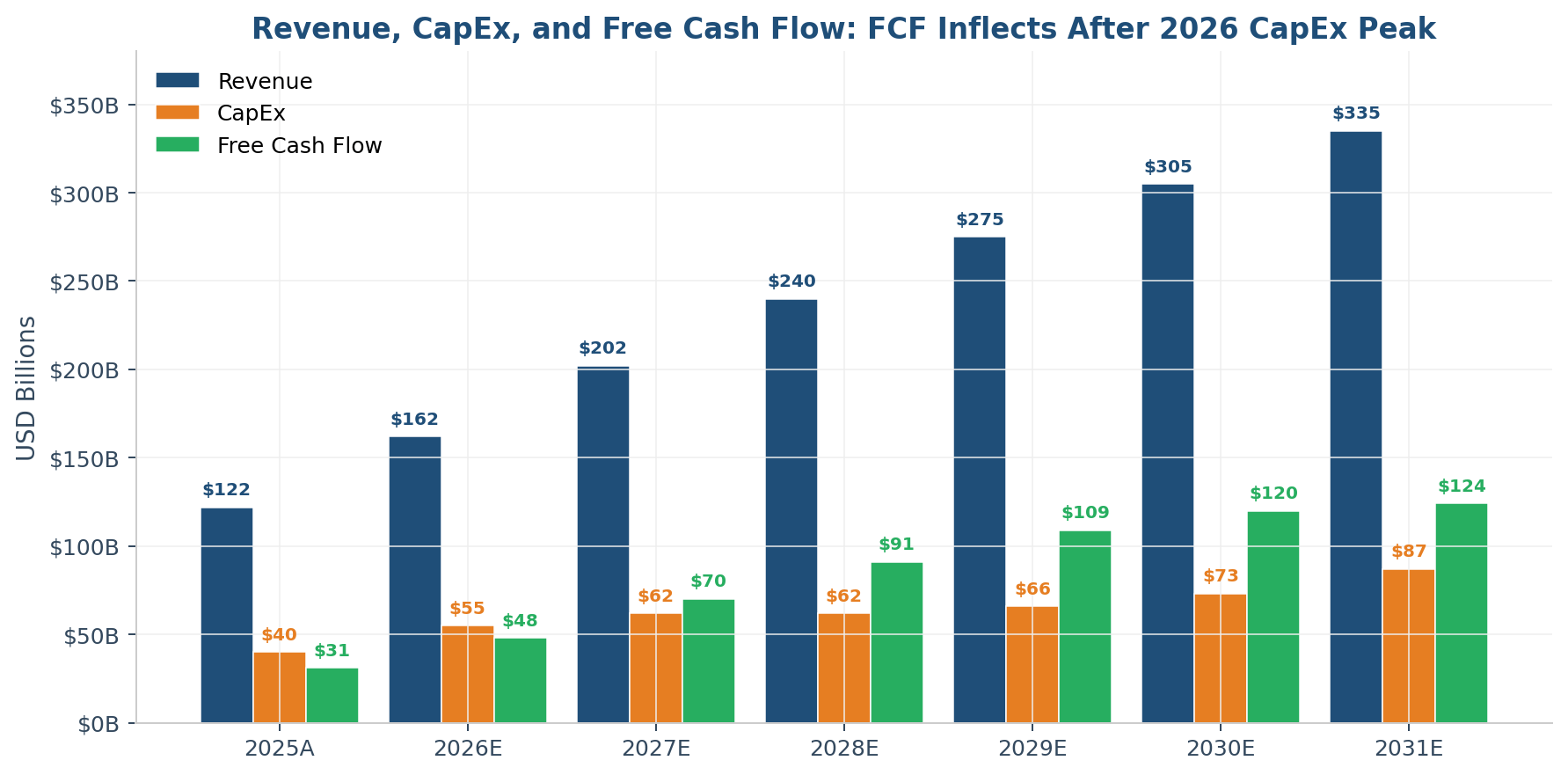
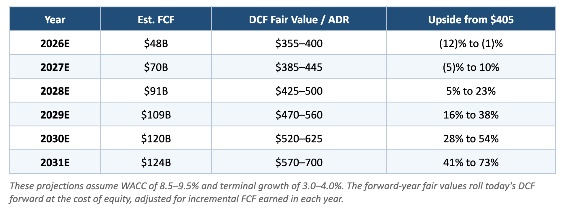
6.3 DCF Results
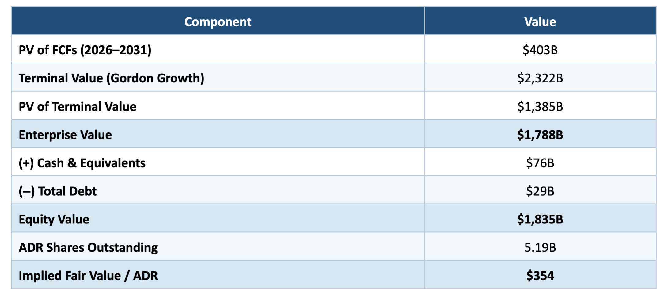
Key Metric: Our base-case DCF yields $354 per ADR versus the current trading price of ~$405 — a roughly 13% discount to spot. The market has moved past the AI-Compute-informed base case and is now pricing a scenario closer to the bull tail (continued AI capex acceleration past 2028, faster Taiwan-risk-premium compression than we model).
This is a meaningful shift. As recently as late 2025, the stock traded near our base-case fair value. The Q1 2026 print — 66.2% gross margin, +40.6% YoY revenue, and management's confirmation that 2nm bookings extend to 2028 — has rerated the multiple. To underwrite a long position from current levels purely on a DCF basis, you need to either bridge to a 4.0–4.5% terminal growth rate (which assumes structural-AI-winner status indefinitely), or accept that 2027–2031 fair-value compounding does the heavy lifting on returns.
6.4 Sensitivity Analysis: Fair Value per ADR
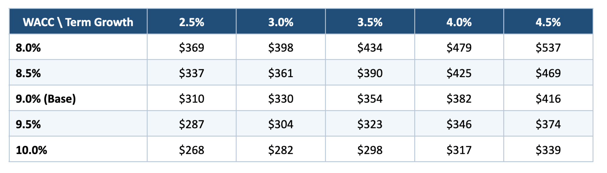
Key Metric: Only the 8.0% WACC row and the 9.0% / 4.5% terminal growth combination ($416) produce a fair value above the current $405 price. The market’s implied WACC × terminal growth combination appears to be approximately 8.0–8.5% × 3.5–4.0%, signaling that investors are now pricing TSMC closer to a structural-AI-winner profile than a cyclical foundry.
7. Projected Fair Value: 2027-2031
As TSMC's free cash flow compounds through the AI investment cycle, the rolling DCF fair value expands materially. The heavy 2026 capex period temporarily compresses FCF relative to earnings, but the recovery into 2028–2031 is substantial.
8. Valuation: Price/Earnings (P/E) Framework
8.1 Methodology
TSMC currently trades at approximately 34.14x trailing twelve-month earnings and ~25x forward 2026 consensus EPS. The 10-year average forward P/E is roughly 18x; the 5-year average is roughly 22x; the post-AI (2023+) average is roughly 26x. We view the rerating as partially structural — the business is demonstrably higher-margin and higher-quality than it was a decade ago — and partially cyclical.
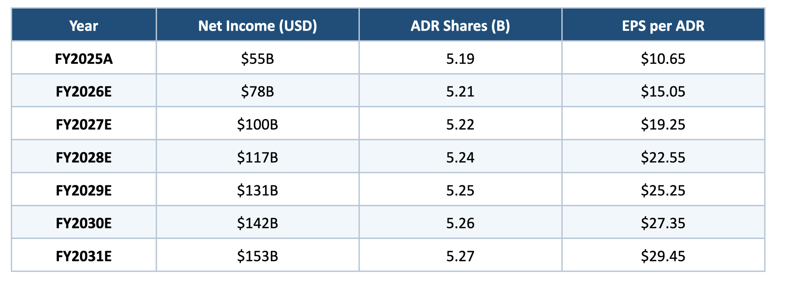
8.2 EPS Projections (per ADR)
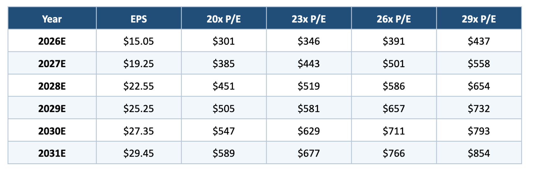
8.3 Implied ADR Price at Various P/E Multiples
8.4 Base Case P/E Targets
Our base case assumes the multiple compresses from ~25x today to ~24x by 2028 and ~23x by 2031.
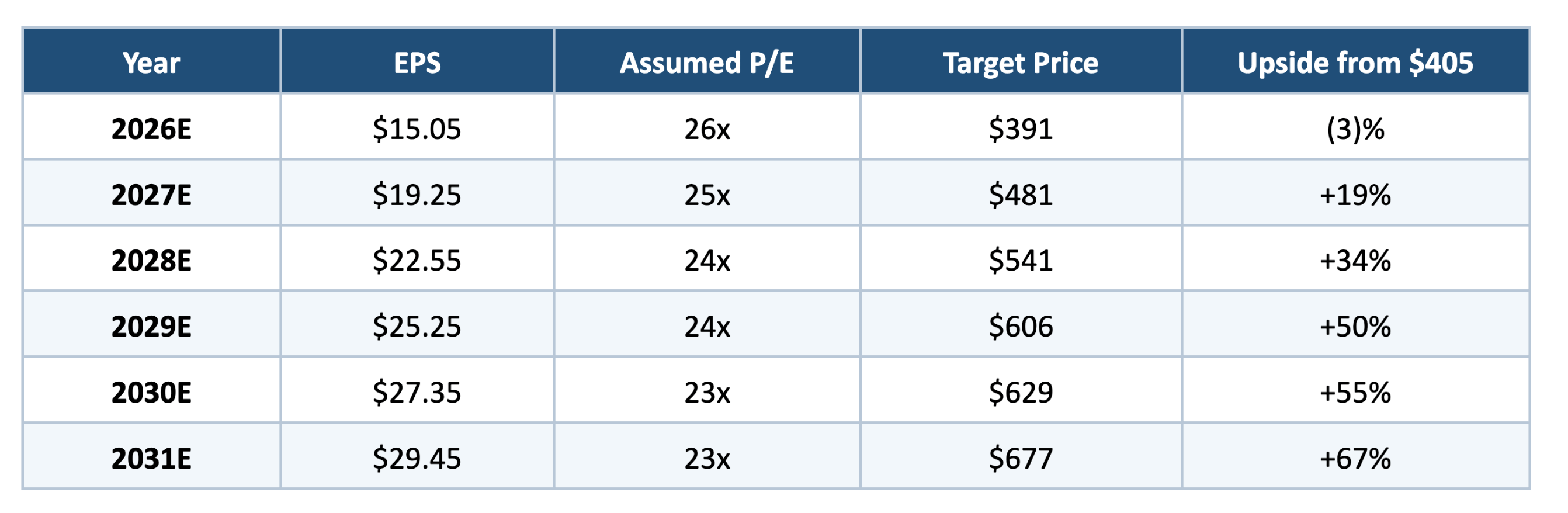
Key Metric: Both the DCF and P/E frameworks converge on a 2031 fair value range of approximately $590–690 per ADR, implying a 5.5-year annualized price return of 7–10% from today’s $405, plus ~1.5% dividend yield for an 8.5–11.5% total return profile.
9. The Bull, Base, and Bear Cases
9.1 Bull Case: $850 by 2031
In the bull case, AI capex continues to compound at 15–20% per year through 2030 rather than decelerating in 2028. Nvidia's Rubin and post-Rubin architectures drive CoWoS-L wafer demand to 200,000 wafers per month by 2028. Operating margins hold above 55% through 2031 because overseas fabs (Arizona in particular) reach parity margins faster than expected as volume ramps. TSMC captures a disproportionate share of agentic/robotic AI silicon demand, which is still almost entirely prospective. Revenue reaches $385B in 2031; net income reaches $177B; EPS per ADR reaches $33.60; the multiple holds at 25x; the ADR trades at $840.
9.2 Base Case: $690 by 2031
This is the projection built above: 2026 grows 33%, growth decelerates to 10% by 2031, operating margins peak at 55.5% and normalize to 52.5%, EPS per ADR reaches $29.45, the multiple compresses to 23x, and the ADR trades at $690. This represents roughly 11.5% annualized total return from $405 (including a ~1.5% dividend yield), which still comfortably beats the S&P 500's long-run return with a modest volatility premium — though the entry multiple matters more from here than it did six months ago.
9.3 Bear Case: $310 by 2031
The bear case is not about TSMC failing to execute; it is about the AI capex cycle rolling over. If hyperscaler capex peaks in 2026 and declines modestly through 2028, HPC revenue growth slows to high single digits. Overseas fab margin dilution turns out to be structural rather than transitional. A Taiwan geopolitical event — even short of invasion — meaningfully reprices the stock. In this case, revenue reaches only $230B in 2031, operating margins fall back to 45%, EPS per ADR is $19.70, the multiple compresses to 16x, and the ADR trades at $315.
9.4 Probability-Weighted Fair Value
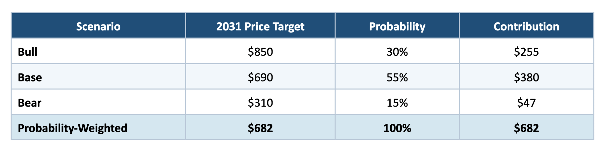
Key Metric: Probability-weighted 2031 fair value of $682 per ADR implies roughly 10% annualized price return from the current $405, with approximately ±$170 of scenario dispersion. Layering the ~1.5% dividend yield brings total return to ~11.5% annualized in the base case.
10. Key Risks
Taiwan Strait Geopolitical Risk. The single most important risk factor, and the one that is hardest to underwrite. A blockade or invasion would cause catastrophic supply chain disruption for the global economy and effectively delete TSMC's equity value in the near term. The US/Japan/Germany expansion described above will reduce single-point-of-failure risk from ~100% in 2023 to ~75% by 2030, but this is a multi-year compression, not an immediate one. The market is implicitly pricing in a roughly 50–100 bps annual risk premium versus otherwise-comparable semi peers — narrowed from ~150 bps two years ago, consistent with the dilution of Taiwan concentration.
AI Capex Air Pocket. Hyperscaler capex has grown from roughly $200B in 2023 to a guided $640B in 2026. At some point this rate of growth decelerates sharply. If the deceleration happens in 2027 instead of 2029, TSMC’s HPC growth trajectory meaningfully disappoints. The risk here is not absolute level of spending (which likely keeps growing) but rate of change. Our AI Compute Demand report estimated the deceleration begins in 2028; an earlier inflection is the primary bear-case catalyst.
Customer Concentration. The top-5 customers will represent 63% of 2026 revenue. A strategic shift by Apple (exploring in-house foundry, deeper insourcing) or Nvidia (second-sourcing to Samsung or Intel) could matter quickly. Neither is probable in the 2–3 year window, but both are not impossible by 2028–2030.
Overseas Fab Margin Dilution. Arizona, Kumamoto, and Dresden fabs are structurally higher-cost than Taiwan fabs. Management has guided 200–300 bps of gross margin dilution through 2027. If dilution is larger or more persistent — particularly if labor cost inflation in Phoenix runs hotter than modeled — the gross margin trajectory disappoints.
Technology Execution Risk. N2 yields, A16 ramp, and CoWoS capacity additions all need to go roughly on schedule. Any material stumble — particularly on A16 given its novel backside power delivery — would cede ground to Intel 18A or Samsung Foundry. TSMC’s execution record is among the best in the world, but the roadmap is getting harder, not easier.
Currency and Export Controls. TSMC reports in NTD but ~90% of revenue is USD-linked; NTD strength (as occurred in late 2025) can compress reported margins. Separately, U.S. restrictions on China-bound advanced semiconductors have not yet meaningfully impaired growth, but any expansion of controls to ≤7nm sales to Chinese firms — or retaliatory Chinese action — would affect 3–5% of revenue.
11. Conclusion
Taiwan Semiconductor Manufacturing Company is, by any reasonable measure, the most important manufacturing company in the world. It is the only entity that can fabricate leading-edge logic at scale; it is the only entity that can package AI accelerators at scale; and it is the only entity whose capital cycle actually constrains the pace of the AI build-out. At $405 per ADR and a $2.10 trillion market cap, the stock is trading at roughly a 13% premium to our base-case DCF fair value — a sign that the market is now pricing a scenario closer to the bull case than the base case. Our base case still produces a $690 ADR price target by 2031 — approximately 10% annualized from current levels, or ~11.5% with the dividend — with bull-case upside to the mid-$800s and bear-case downside to ~$310.
For long-term investors, TSMC is not a cheap stock. It is, however, a uniquely durable asset in a decade where the marginal unit of global economic output increasingly depends on leading-edge silicon. The Morris Chang thesis — that a neutral, focused, open foundry would eventually be worth more than any single integrated device manufacturer — has been vindicated at a scale Chang himself probably did not anticipate. The next decade will test whether it can be vindicated a second time, at even larger scale, through the AI cycle and whatever cycle follows it. The accelerating US, Japan, and Germany build-outs materially reduce the single-point-of-failure discount that once justified a deeper multiple haircut; that compression is a slow-moving but real second tailwind to the earnings story.
Sources
1. TSMC Q1 2026 Earnings – CNBC
2. TSMC Q1 2026 Quarterly Results
3. TSMC Q1 Revenue Tops $35.9bn on 3nm Demand – eeNews Europe
4. Earnings Call Transcript: TSMC Q1 2026 – Investing.com
5. TSMC Q4 2025 Management Report
6. TSMC Board OKs 2025 Results, Dividend, Big Capex
7. TSMC December 2025 Revenue – The Tribune
8. Nvidia Set to Supplant Apple as TSMC’s Top Customer – CNBC
9. Nvidia Overtakes Apple as TSMC’s Biggest Customer – MacRumors
10. TSMC Client Rankings Shake Up by 2026 – SMBOM
11. TSMC 2nm Mass Production – FinancialContent
12. TSMC 2nm First Customers: Apple, AMD, NVIDIA, MediaTek – Design-Reuse
14. TSMC A16 Super Power Rail Announcement – AnandTech
15. TSMC CoWoS Capacity to Reach 130,000 Wafers Monthly
16. Nvidia Secures 60% of CoWoS Capacity – Astute Group
17. CoWoS Capacity – DigiTimes
18. Morris Chang: Foundry Father – IEEE Spectrum
19. The Silicon Empire: TSMC’s Revolution – Quartr
20. How Taiwan Came to Dominate the Global Chip Industry
21. TSMC Ups Revenue Guidance and CapEx – Tom’s Hardware
22. TSMC Arizona $165B Expansion
23. TSMC 2nm Orders Run to 2028 – Paradox Intelligence
24. Apple’s A20 Chip Breakthrough – AppleMagazine
25. TSMC Stock Price and Valuation Data – Companies Marketcap
26. TSMC Japan (JASM) Kumamoto Operations – Sony
27. TSMC Germany (ESMC) Dresden Construction – Reuters
Disclaimer: This report is for informational and educational purposes only. It does not constitute financial advice, and the projections herein are estimates based on publicly available information and the author's analysis. Past performance does not guarantee future results. Always conduct your own due diligence before making investment decisions.